


The Representative Office in New Delhi of the Japan Bank for International Cooperation (JBIC), jointly with other institutions, held the third meeting of the Semiconductor Committee of the Japan Chamber of Commerce and Industry in India (JCCII) and a site visit tour of Dholera Industrial Area for the member companies of the committee. The committee itself was launched in April 2024 at the initiative of the government and governmental institutions of Japan with the objective of promoting Japanese semiconductor companies in entering in India and contributing toward the realization of cooperation between Japan and India in the semiconductor sector. The secretary general of the committee is Chief Representative KURIHARA Toshihiko of JBIC’s Representative Office in New Delhi.
The secretariat of the committee includes the Embassy of Japan in India, the Ministry of Economy, Trade and Industry, the Japan External Trade Organization (JETRO), and the Japan International Cooperation Agency (JICA). In addition, as many as 110 companies have already joined the committee, including not only semiconductor parts manufacturers and semiconductor manufacturing equipment makers, but also companies from diverse sectors involved in the semiconductor supply chain, such as logistics, construction, electricity, and gas.
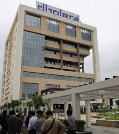
On September 5 and 6, JBIC held with JETRO a site visit tour of Dholera Industrial Area. Dholera is the most critical area in the Delhi Mumbai Industrial Corridor project promoted by the National Industrial Corridor Development Corporation (NICDC), which supports the development of industrial corridors throughout India. JBIC has been involved in the development and operation of the industrial area through partial investment in NICDC. The first day of the tour started with keynote speeches. Mr. Manish Gurwani, Mission Director of Gujarat State Electronics Mission (GSEM) and Mr. Kuldeep Arya, CEO of Dholera Industrial City Development Limited (DICDL) talked about the investment promotion policy related to semiconductor business in Gujarat State, the region highly expected to play a central role in the ecosystem of India’s semiconductor industry. Then DICDL presented on the development status of the industrial area and guided the participants through the industrial area, including a factory tour at Renew, a solar panel manufacturer. During this tour, the participants showed a high level of interest in collaborating with India in the semiconductor sector and expanding into the industrial area.
Mission Director of GSEM
CEO of DICDL
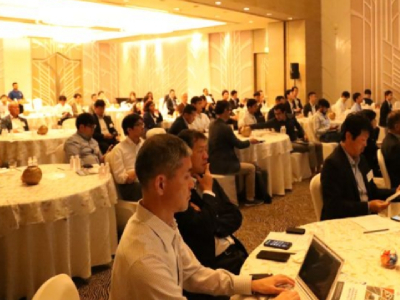
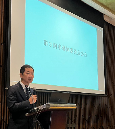
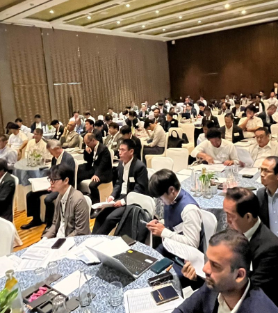
On September 10, JBIC and JCCII co-hosted the third meeting of the Semiconductor Committee. After the opening remarks by Mr. MATSUO Takehiko, Vice Minister for International Affairs at the Ministry of Economy, Trade and Industry (METI), presentations were given by Ms. Ritika Singh, Head of Fab Strategy and Planning of TATA Electronics Private Limited, a subsidiary of Indian giant TATA Group and Mr. Jerry Arucan Agnes, CEO of CG Semi Private Limited, which is a semiconductor arm of industrial conglomerate Murugappa Group. During the sessions, presenters and participating companies actively exchanged opinions regarding the business strategies of Japanese companies in India and future collaboration between Japan and India.
Then, Mr. MATAUNO Issei, from JICA India Office, made a presentation about research on semiconductor sector and Ms. SAKUMA Kazuko, Resident Executive Officer, Regional Head for Asia and Pacific of JBIC introduced the progress of development of Dholera Industrial Area and JBIC’s support system.
The meeting attracted nearly 110 participants from the governments, governmental agencies, and private companies of both countries, providing them with opportunities to exchange opinions and network.
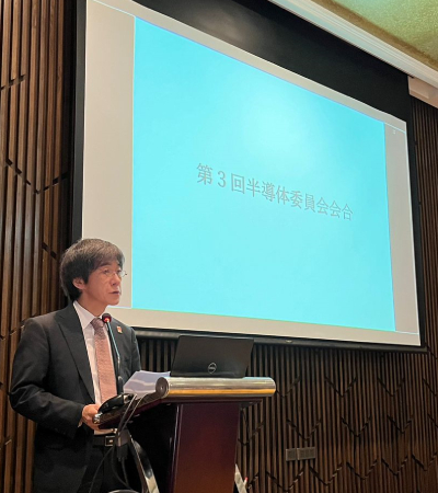
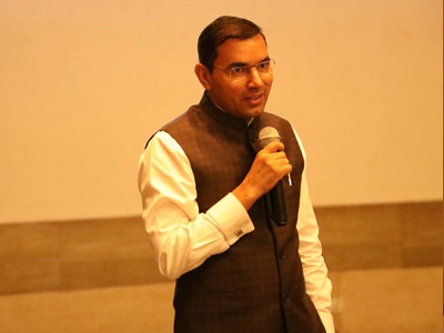
Vice Minister for International Affairs at METI
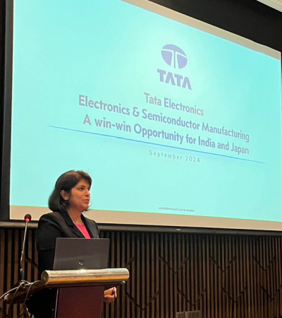
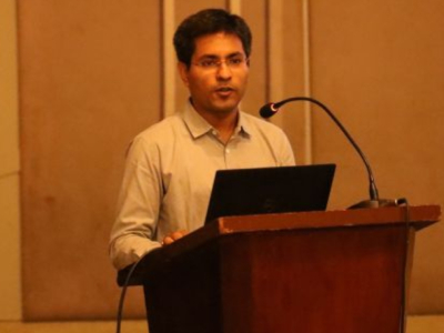
Head of Fab Strategy and Planning of TATA Electronics Private Limited
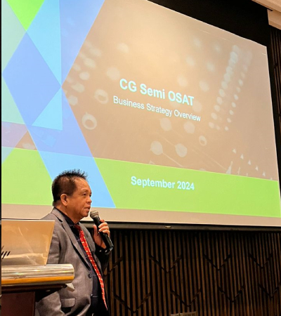
CEO of CG Semi Private Limited
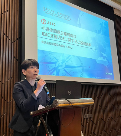
Resident Executive Officer, Regional Head for Asia and Pacific of JBIC
Chief Representative of JBIC Representative Office in New Delhi
As Japan's policy-based financial institution, JBIC will continue to actively support the creation of business opportunities and the promotion of business for Japanese companies and contribute toward the further development of economic relations between related countries by collaborating closely with overseas governments.
Note
- *1
GSEM was set up to focus on creating a dynamic ecosystem for electronics, semiconductors, and display manufacturing.